Disclaimer : All the articles are written with an assumption
that the reader has a basic knowledge of Boolean Gates and digital elements.
In this article, the key focus of discussion would be clock
gating and its impact on the design on modern day SoCs. Clocks could be
considered as the Arteries (or Veins so for the matter) of the entire SoC and
clock source being the heart of any SoC. All the IP’s like CPU, Audio, Display,
USB, etc require a clock to function. It is the “CLOCK” which gets to decide
the maximum speed of operation for any SoC (Here I am not considering the
throughput increase due to the various kinds of architectures employed in
designing the SoC) and hence special attention should be given to this signal.
Another reason why this signal should be given more attention
is due the fact that it is the highest toggling signal in any SoC and therefore
consumes the largest fraction of entire SoC power. In a typical SoC for mobile
application, the clock tree consumes 30-40% of the power (Yes, this number can
be more depending on the Clocking architecture employed).
Clock gating is a technique to turn the clock OFF depending
on the requirement or the use case. How this is achieved is the main focus of
this topic.
There are essentially two ways to gate the clock. One through
hardware control and one through software control.
The software control is through registers which are used to
control the PLL or DLL or any other clock source that we may have. We turn the
PLL/DLL/Source off (which is in itself at times a complex process) by following a
specific sequence. Turning of the source is a method to gate the trunk of the
clock tree (I’ll talk about the Industry lingo on clocks in an upcoming
article. Kindly bear with us on terms like trunk, branch, etc).
It may happen that in some of the cases we want to shut only
a branch of the trunk. This is the point where hardware control comes in
picture.
This article (and some subsequent articles) will discuss on
hardware control of the clock.
Below is shown a free running clock :

Fig 1. Free Running Clock
---------------------------------------------------------------------------------------
How can we actually stop it based on some control signal say “enable”?
How can we actually stop it based on some control signal say “enable”?
---------------------------------------------------------------------------------------
Yes, you got it right, we need to AND the two signals and put
the enable to be at “1” when we need the clock and “0” when we don’t want the
clock output for any IP.
The figure below shows a simple AND gate being used as a gate.
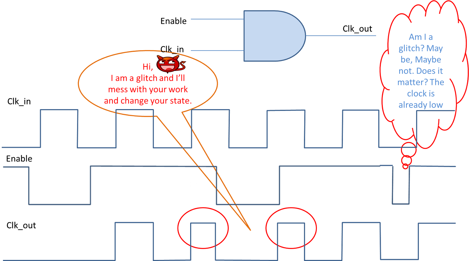
Fig 2. AND Gate as a Clock Gate and Problem of Glitch
So do we actually use this “AND” gate in our SoCs to gate the
clock from reaching to any IP?
You guessed it right. No, this is not the standard cell which
any modern day SoC use. The reason is clear from above figure itself. If the
enable signal changes while the clock is high, this will lead to a runt pulse
termed as “Glitch”. A glitch is harmful for any SoC as it can lead to unknown
states or the states which we don’t want our system to be in. For now, I’ll
leave the glitch to a-not-so-far-in future article.
I’ll discuss about “Clock Gating Cell” in the next article.
Till then, Enjoy!!!
No comments:
Post a Comment