Moving ahead from my last article
on Clock gating(You can read the previous article here : Low Power Techniques - Clock Gating), this small article introduces the standard “Clock Gate Cell”
This cell is available to all the designers in semiconductor industry along with the other standard cells in their libraries. It is good to recognize early that clock and power are mingled up and clocks provide a good deal of avenues for saving power. So knowing more about clocks is always a plus to person interested in designing "Power Aware Circuits".
In the last article, we saw that
there was a glitch in “certain cases”, when we gated the clock. These “certain
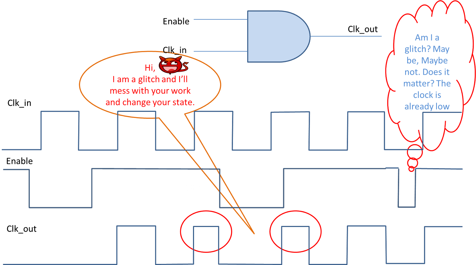
cases” led to the development of this cell. If you look more closely at the
waveform given in last article (reproduced below for convenience), the glitch
will always be there whenever the enable signal goes down and the clock is
high (high as in logic 1) .

Fig 1. AND Gate as a Clock Gate and Problem of Glitch (Reproduced from Low Power Techniques- Clock Gating)
The above observation is simple enough to propose a
solution for the glitch problem in AND gate. Fig 2. shows the clock gate cell.

Fig 2. Clock Gate Cell
This
cell stops the clock without any glitch in the output. And how does it do that? It utilizes a LATCH for
this purpose.
-----------------------------
Latching Mechanism
-----------------------------
A latch is a level sensitive device in which the output is same as input till its Enable signal is at a particular logic level. Generally logic 1 is the chosen level for this matter. The output traces the input till the Enable signal is logic 1 and as enable is switched to logic 0, the output retains the last value it captured from the input till the next enable comes where it starts tracking the input again.
------------------------------------------------------------------
Latching Mechanism as used in Clock Gate Cell
------------------------------------------------------------------
For clock gating purpose the enable signal of latch is tied to the inverted clock signal (Clk_in) so that output
changes only when the clock is at a particular logic level (which is logic 0 in our case). So it
is easy to see that we can pass Enable signal and the changes will be recorded only when the logic level is low (or logic 0) and then AND this with
the clock signal. This will ensure that that the Enable low is recorded only
when the Clk_in is low and hence no glitch in the output.
Note that we have inverted the
clock before sending it to the latch so as to ensure that the latch is
sensitive to logic 0 of Clk_in (since the latch itself is sensitive to logic 1).
Before I proceed further, I would like to point out that a latch is a very
powerful tool available to designers and it is used in multiple circuits (it will
be a hot topic in some of the coming articles). With above cell Fig 1. modifies to Fig 3. as below :

Fig 3. Timing Waveform for Clock Gate
In the above figure notice how the enable edges which happened during the clock high have been translated or rather delayed in the clock low domain.
We can use this cell to TURN OFF an entire
clock domain or TURN OFF only a few flops. It is entirely on designer that how much
power he wants to save and according to that we have levels of clock gating in
any SoC. Also note that these Enable signals are controlled by Finite State
Machines (FSMs) which trigger based on inputs from other FSMs in SoC.
A small point to all the above
information is : Clock gate is a HW means to control the clock signal there
are software means as well in which we program the PLL itself to control the
entire clock tree.
I conclude this article here with these lines of Dr. Thomas Fuller :
"Let not thy will roar, when thy power can but whisper"