Wednesday, 11 March 2015

Online course on "Computing Technology"

For all the computer enthusiasts (and those who want to learn about the basics of computer design), there is an online course which started recently. It covers most of the basics of processor design starting from digital electronics till the programming end(the different layers of development and also the various jobs that are built around those layers :) ).

The link to the course is  : The Computing Technology Inside Your Smartphone

The course, though may be named as the "The Computing Technology Inside Your Smartphone", covers the fundamental of computer architecture with the case study of Qualcomm's Snapdragon processor which is used in plethora of smartphones in modern day(Smartphones from a wide range of companies like Samsung, HTC, Lenovo, Xiomi, etc use Qualcomm's snapdragon SoC{SoC is semiconductor industry jargon for System-on-Chip} ).

Kindly enroll in this course as it starts from the basics and gives out a strong idea about how such a large computer (from the PC era) has shrunk to size where it can be accommodated in our pockets(the smartphone era).

Even if you do not know anything about the electronics, this course can definitely help lay a foundation of electronics. Moreover you will be designing one such processor yourself.

Cheers !!!
Happy Learning !!! :)


Friday, 6 March 2015

Video Series on "Foundation of Computer Science"

It has been a long time since we were last active on the blog. Kindly accept our apologies for that as we have been a lot busy with our work life, but we are back and as mentioned in our last post that we would be providing some useful links to build upon your knowledge in various domains of electronics and computer science, here are the few good links for learning more about these fields :

If you want to learn about Foundations of Computer Science you can join the courses offered by MIT (Massachusetts Institute of Mechnology) under edx/Xseries section. About the courses in Foundation of Computer Science (quote from the xseries itself : https://www.edx.org/xseries ) :

"The Foundations of Computer Science XSeries, offered by the M.I.T. Department of Electrical Engineering and Computer Science, is a sequence of courses that introduce key concepts of computer science and computational thinking. Students apply these concepts and build their engineering skills by completing software and hardware design problems. Additionally, students test their understanding by taking a series of exams"

Though there are seven courses in the series, these cover a good amount of Digital Electronics as well.
Currently two of the 7 courses are ongoing(started this Monday and Tuesday) and you can enroll in them to learn the basics of Digital Design and computer science concepts using Python.

Here are the links to those :

1. 6.00.2x Introduction to Computational Thinking and Data Science
2. 6.004.1x Computation Structures: Digital Circuits 

It is not mandatory for you to join the courses with the fees, you can also pursue the course freely by signing up for the honor code certificate. All you need is an internet connection.

I will keep updating when other courses of the series start.

If you have any doubt regarding what all courses(related to the field of Electronics or Computer Science) to do you can comment here, for queries related to the above courses you can ask them in the discussion forums (or here as well)

Till then, happy learning. :) 

Wednesday, 1 October 2014

Message from SOCD Team

Hi All,

After an overwhelming response from people who want to learn the basics of electronics and are in search of resources for learning new things in the area of SoC design, we thought that it would be a good idea to pour in a basic learning curve for all the "Electronics Enthusiasts". Motivated by the appreciative response from people, we have added another menu button which will contain links to various important lectures which can be used as a road-map for learning the basics of SoC design and related fields.


Under Video Tutorials tab above you will find blogs which will contain links to various courses that can be undertaken to learn SoC design, starting from scratch. Also this section will contains links to videos in various fields of SoC design and application including VLSI Digital design, Computer Architecture, Analog Design, Embedded systems, languages like Verilog/System Verilog, etc.

We do not guaranty that you will become instant success after going through the videos, but we do guaranty that given proper amount of time, one can become a virtuoso of the field the person chooses to work on. It will take time but the time spent will be highly rewarding and lead to a start of new learning curve on which you can build upon.

Also these lectures (if the mentioned pattern is followed) will be helpful when you join the industry of your preference (these will be helpful in your interviews as well). We found these lectures awesome and highly satisfying, hope they do the same for you. With the Semiconductor market being highly competitive, it is really difficult for a fresher to land a job in the Industry, but with proper planning and using the correct resources there are vast amount of opportunities in the field. In fact most of the companies have so many vacancies but they are not able to find the appropriate talent among a large pool of Electronic Engineers because of lacking the appropriate knowledge and basic skill set.

Putting these tutorials together(and the blogs) is our means of providing the knowledge which is relevant for any candidate which is aspiring to land a job in the Semiconductor Industry.

Hope all the effort will be really helpful for the learners !!!

Kindly like the facebook page of the blog for getting updates. The link is provided below :

                                                                       SoC-ASIC-Design Facebook Page

or you can subscribe the blog by clicking on the subscribe option in the right side of the window.

Till the next post.

Cheers !!!!

SOCD Team

Saturday, 13 September 2014

Standard Clock Gate Cell

Moving ahead from my last article on Clock gating(You can read the previous article here : Low Power Techniques - Clock Gating), this small article introduces the standard “Clock Gate Cell” This cell is available to all the designers in semiconductor industry along with the other standard cells in their libraries. It is good to recognize early that clock and power are mingled up and clocks provide a good deal of avenues for saving power. So knowing more about clocks is always a plus to person interested in designing "Power Aware Circuits".

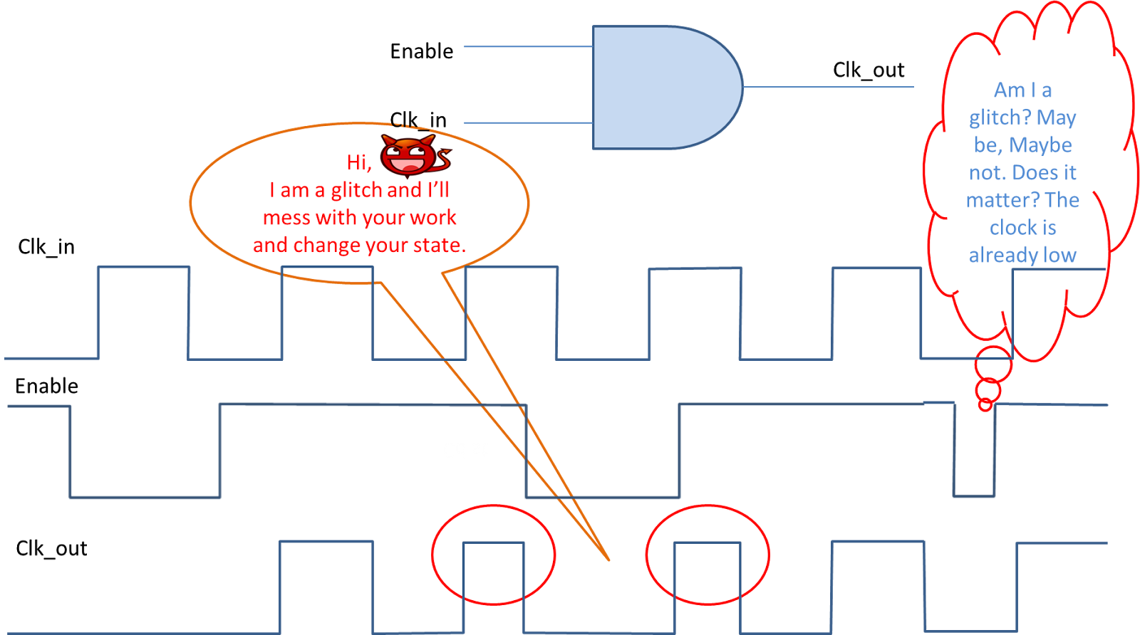
In the last article, we saw that there was a glitch in “certain cases”, when we gated the clock. These “certain cases” led to the development of this cell. If you look more closely at the waveform given in last article (reproduced below for convenience), the glitch will always be there whenever the enable signal goes down and the clock is high (high as in logic 1) .
Fig 1. AND Gate as a Clock Gate and Problem of Glitch (Reproduced from Low Power Techniques- Clock Gating)

The above observation is simple enough to propose a solution for the glitch problem in AND gate. Fig 2. shows the clock gate cell. 
Fig 2. Clock Gate Cell


This cell stops the clock without any glitch in the output.  And how does it do that? It utilizes a LATCH for this purpose. 

-----------------------------
Latching Mechanism
-----------------------------
A latch is a level sensitive device in which the output is same as input till its Enable signal is at a particular logic level. Generally logic 1 is the chosen level for this matter. The output traces the input till the Enable signal is logic 1 and as enable is switched to logic 0, the output retains the last value it captured from the input till the next enable comes where it starts tracking the input again.

------------------------------------------------------------------
Latching Mechanism as used in Clock Gate Cell
------------------------------------------------------------------

For clock gating purpose the enable signal of latch is tied to the inverted clock signal (Clk_in) so that output changes only when the clock is at a particular logic level (which is logic 0 in our case). So it is easy to see that we can pass Enable signal and the changes will be recorded only when the logic level is low (or logic 0) and then AND this with the clock signal. This will ensure that that the Enable low is recorded only when the Clk_in is low and hence no glitch in the output.

Note that we have inverted the clock before sending it to the latch so as to ensure that the latch is sensitive to logic 0 of Clk_in (since the latch itself is sensitive to logic 1). Before I proceed further, I would like to point out that a latch is a very powerful tool available to designers and it is used in multiple circuits (it will be a hot topic in some of the coming articles). With above cell Fig 1. modifies to Fig 3. as below :

Fig 3. Timing Waveform for Clock Gate

In the above figure notice how the enable edges which happened during the clock high have been translated or rather delayed in the clock low domain.

We can use this cell to TURN OFF an entire clock domain or TURN OFF only a few flops. It is entirely on designer that how much power he wants to save and according to that we have levels of clock gating in any SoC. Also note that these Enable signals are controlled by Finite State Machines (FSMs) which trigger based on inputs from other FSMs in SoC.


A small point to all the above information is : Clock gate is a HW means to control the clock signal there are software means as well in which we program the PLL itself to control the entire clock tree. 

I conclude this article here with these lines of Dr. Thomas Fuller :
"Let not thy will roar, when thy power can but whisper"

Tuesday, 2 September 2014

Low Power Techniques : Contemporary Strategies - I

Most of the SoC designs for mobile domain(by Mobile Domain, I mean the devices being used in SmartPhones, tablets, laptops, or any gadget which can be carried from one place to another easily) require it to consume low power while performing operations at the same time.


This article discusses the various contemporary techniques (in brief) employed by the Design companies in coming up with such complex SoCs. Before we proceed any further, I would like to differentiate between two terms which are often used interchangeably in the industry these days. They are : Low Power and Power Aware

There is a difference in the two terms which I mentioned above. Be known that “Low Power is not the same as Power Aware.”

Difference between Low Power and Power Aware Techniques

Low Power (in the context of these devices) means that the device will consume low power owing to the way it is implemented. One example for this would be the use of High Threshold (High Vth) MOS transistors in the design which has lesser leakage and performs slower than the Low Vth transistors which are leaky.

Power Aware, on the other hand, implies that the SoC or device itself is intelligent enough to shut down or turn-off the units which are not required while performing a particular operation or the device knows when to operate at a lower frequency or in a low power consuming mode/state.

Contemporary SoCs are a mingled version of Power Aware as well as Low Power Techniques to have an optimum performance and power consumption at the same time. Due to excessive power consumption by these small devices, a new parameter has emerged as a metric for SoCs. It is Performance per Watt or in Industry Lingo it is Perf/Watt. Know that this number will be different for different types of tests/benchmarks we run on the design. Generally the worst case Perf/Watt should be reported.
So here I go on listing and summarizing the techniques that are being used.

I leave it to you to categorize the technique as low power or power aware. J

The first and simplest to understand is MTCMOS

1.      MTCMOS (Multi – Threshold CMOS)
Fig 1.  Types of MOS Transistors with different Vt

 As mentioned above, this technique is highly useful in reducing leakage power. Every company has its own standard cell library and a standard library is provided by “The Foundry” as well. This library (the one provided by the foundary) contains transistors with varying thresholds or different Vth’s. Since low Vth implies(these cells are termed as LVT cells; LVT standing for Low Vth) higher leakage but high speed, we tend to use them in timing critical paths (What is a timing critical path??) or in other words, the path which has the largest delay (arising from flops, combo logic) in it. For all other paths or in between logic, we use the cells with medium Vth(SVT for Small Vth) or high Vth(HVT for High Vth) which has lower performance but are highly tolerant to leakage power. In fig 1b., the solid dashed line in the gate is used to depict that it is a high threshold device. The Vth of the transistor is changed by varying the oxide (SiO2) thickness in the MOS transistor and hence the solid line for showing thick oxide layer in fig 1b. 
For details you can visit this article again :  Basics of MOS Devices 

2.      Multiple Supply Voltages

Fig 2. A SoC with Multiple Voltage Islands

Kindly note that above figure is arbitrarily drawn and bears no resemblance to any existing SoC. 
For a long time the industry has been dreaded by the dynamic power consumption which is a strong function of the operating voltage, frequency and load capacitance, given by the relation :

Pdyn = CLVDD2f
Note that in above equation I have not considered the switching factor.
As per above equation if we reduce the operating voltage by 2 by keeping all the other things constant, the dynamic power would be reduced by a factor of 4. This simple approach is used in coming up with SoCs which have different voltage islands in it. The different parts of the SoC operate on different voltages, and of course on different frequencies. As an example the audio unit in any SoC can operate at lower frequency than the display unit and hence we can use different voltages for these two types of IP’s. Such scenario is depicted in figure above.

I’ll talk about more about the remaining techniques in a follow - up article.

Till then, “It is not the end but a start of new era of revolution”.

Saturday, 30 August 2014

Low Power Techniques : Clock Gating

Disclaimer : All the articles are written with an assumption that the reader has a basic knowledge of Boolean Gates and digital elements.

In this article, the key focus of discussion would be clock gating and its impact on the design on modern day SoCs. Clocks could be considered as the Arteries (or Veins so for the matter) of the entire SoC and clock source being the heart of any SoC. All the IP’s like CPU, Audio, Display, USB, etc require a clock to function. It is the “CLOCK” which gets to decide the maximum speed of operation for any SoC (Here I am not considering the throughput increase due to the various kinds of architectures employed in designing the SoC) and hence special attention should be given to this signal.

Another reason why this signal should be given more attention is due the fact that it is the highest toggling signal in any SoC and therefore consumes the largest fraction of entire SoC power. In a typical SoC for mobile application, the clock tree consumes 30-40% of the power (Yes, this number can be more depending on the Clocking architecture employed).

Clock gating is a technique to turn the clock OFF depending on the requirement or the use case. How this is achieved is the main focus of this topic.


There are essentially two ways to gate the clock. One through hardware control and one through software control.

The software control is through registers which are used to control the PLL or DLL or any other clock source that we may have. We turn the PLL/DLL/Source off (which is in itself at times a complex process) by following a specific sequence. Turning of the source is a method to gate the trunk of the clock tree (I’ll talk about the Industry lingo on clocks in an upcoming article. Kindly bear with us on terms like trunk, branch, etc).
It may happen that in some of the cases we want to shut only a branch of the trunk. This is the point where hardware control comes in picture.

This article (and some subsequent articles) will discuss on hardware control of the clock.

Below is shown a free running clock :


Fig 1. Free Running Clock
---------------------------------------------------------------------------------------
How can we actually stop it based on some control signal say “enable”?
---------------------------------------------------------------------------------------

Yes, you got it right, we need to AND the two signals and put the enable to be at “1” when we need the clock and “0” when we don’t want the clock output for any IP.
The figure below shows a simple AND gate being used as a gate.


                                       Fig 2. AND Gate as a Clock Gate and Problem of Glitch

So do we actually use this “AND” gate in our SoCs to gate the clock from reaching to any IP?

You guessed it right. No, this is not the standard cell which any modern day SoC use. The reason is clear from above figure itself. If the enable signal changes while the clock is high, this will lead to a runt pulse termed as “Glitch”. A glitch is harmful for any SoC as it can lead to unknown states or the states which we don’t want our system to be in. For now, I’ll leave the glitch to a-not-so-far-in future article.

I’ll discuss about “Clock Gating Cell” in the next article.


Till then, Enjoy!!! 

SESSION 3: Reading from FG-MOSFETs: Part- 1

Hello everyone. In previous sessions, we have discussed the method to program and erase an FG-MOSFET. 

And programmed state corresponds to binary 0, whereas erased state corresponds to binary 1.

Now the question here lies: how will you get to know whether your FG-MOSFET has a binary '0' or a binary '1' stored in it? In other words, how will you read the data present in FG-MOSFET?

------------------------------------------------------------
The answer lies in the threshold voltage.
------------------------------------------------------------

Now suppose I connect an FG-MOSFET to two batteries, one VGS between gate and source, and the other VDS between drain and source. See the figure below.


So the voltage VGS provides an electric field in the direction shown by the red arrows in the figure below:

Because of this electric field, the holes at the interface of p-type semiconductor and oxide layer are repelled away. The electrons appear at this interface from bulk of p-type semiconductor, thus forming an n-type channel between n-type source and n-type drain. Since this n-type channel is formed from p-type semiconductor, it's called inversion channel.

What role does VDS play here? It provides the field from Drain to Source, thus pulling electrons from Source to Drain via the inversion channel formed by applying VGS. 

You may visualize the above process in the video below. The small red circles represent the holes in p-type semiconductor and the small green circles represent the electrons. Note the inversion channel formation in the video.


In the above video, the flow of electrons indicates the flow of current in external circuit. 
Now, what if the voltage VGS  was not sufficient enough to create the inversion channel? Then obviously, current will not be able to flow.So for every FG-MOSFET, there is a particular value of VGS, only above which the inversion channel is formed and conduction takes place. This value is called threshold voltage, VT.

So, the conclusion till now is: 

The following graph represents the above relation between current IDS and VGS:


As we might intuitively conclude that increasing VDS shall also increase the current IDS (the greater the VDS, greater the pull on electrons via the channel), but does it go on forever?
Reason: Channel pinch-off

Let us see what is channel pinch-off and why does it occur in the next part of this session.
Eventually you will see these concepts clubbing together to build up the concept of reading from an FG-MOSFET.


Till then : "Thresholds are not the ends! Something definitely lies beyond them"